Introduced in 1995, formally discontinued in 2002, but revived in 2003. You might be surprised to learn that its legacy still lives on to this date, but maybe not how you might expect.
Ahead of its time: the Pentium Pro
The Pentium Pro signed the start of a great series of success for Intel and most of its technological enhancements are still living on in modern CPUs designs.
For the mainstream home user, the Pentium Pro meant close to nothing. This first iteration of the P6 core was born as the successor of the “classic” Pentium, but it was focused mainly to the professional and server market. This bias towards high-performance applications and 32-bit operation impacted on 16-bit performance, but the then brand-new Windows 95 still relied on the ageing 16-bit DOS kernel, rendering the CPU less than ideal for home use.
Among the plethora of technical improvement in the main processing core, what stood out were the introduction of out-of-order and speculative execution, on-chip L2 cache and native multi-processor support.
The first two were helped by a longer pipeline with new stages being dedicated to x86 instruction decoding, translation and reordering: the P6 core used an internal reduced instruction set, stored as microcode on the CPU itself, which was used to translate direct x86 machine code to a more manageable instruction sequence.
Second level cache used to live on the motherboard, if present at all: despite not being on-die due to manufacturing issues, it gave a major boost in performance by providing an additional layer of fast volatile storage between the CPU and the system bus, while also reducing latency.
Multi-processor systems lived only in the high-end workstation and server market by providing up to four-way processing on a single board: it still was quite far from the modern concept of multi-core, but *nix, OS/2 and Windows NT had dedicated kernels with scheduler optimizations for systems with more than one processing unit, thus allowing real parallelization.
Speculating performance
Something might have rang a bell in your head: speculative execution. In 2018, Intel announced the discovery of major security flaws regarding this exact part of their processors architecture, but the patches were infamous to hit system performance quite hard. The technology might have had unforeseen consequences, but the actual performance boost it gives is extremely helpful. At least for some extent…
Speculative execution renders the entire x86 platform fast as it is by speculating what the next instruction will be, executing it right away and storing the results in cache: if the speculation is correct, everything is fine and continues as is, otherwise the entire pipeline has to be flushed and refilled with the correct instructions and data, costing an amount of clock cycles equal to the pipeline stages. This last bit is part of the key of the success for P6 and the cause of doom for NetBurst.
Going forward: Pentium II and Pentium III
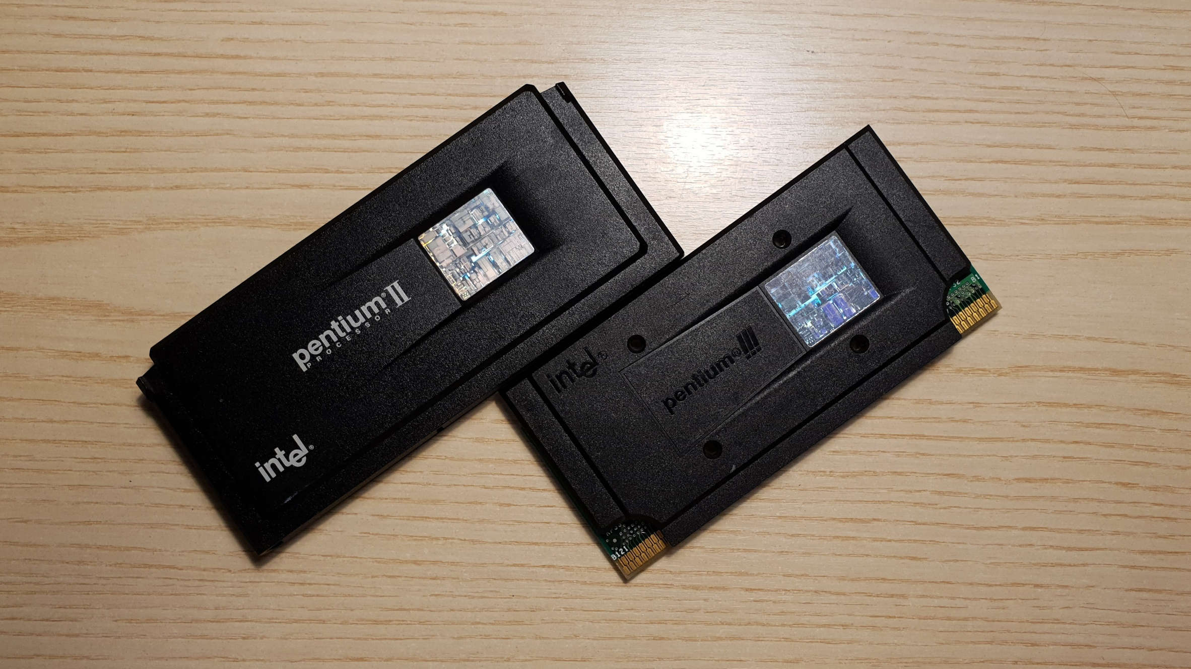
The professional playground paid off: the architecture got all the refinements needed to be marketed as a consumer product and to become a striking success.In 1997, the release of the Pentium II marked the entry of P6 in the mainstream market, by fixing 16-bit performance (absolutely necessary for the popular Windows 9x series) and improving bus and core clock speeds with a finer manufacturing process and lower voltage. CPUs were now in a new package, using a cartridge instead of the classic socket: the main reasons for this choice were better production yields, by not having to hardwire the cache directly to the silicon die, but using a printed circuit board to interface them, and easier replacement on the mainboard by not having to remove the heatsink to reach the CPU.
The years 1999 and 2000 saw one of the greatest peaks of CPU technology, particularly regarding core clocks. The Pentium III lineup saw models ranging from 450 MHz up to 1.4 GHz, making clear what could be done with this architecture: overall performance was made even better by on-die L2 cache, running at full core speed, Front Side Bus up to 133 MHz, improved branch prediction and a slightly longer pipeline. The Slot 1 interface wasn’t the best way to keep up with higher frequencies and power draw, as signals struggled to come across untouched. The PGA370 socket stepped in and standard sockets became the norm again.
The Pentium III also had the so-welcome introduction of the Streaming SIMD (Single Instruction, Multiple Data) Extensions. SSE instructions helped with the more demanding multimedia workloads by reusing the same microcode to process more data, without having to reload instructions again and losing precious cycles. To this date, SSE received numerous revisions and only since late 2016 Advanced Vector eXtensions started to replace SSE for the heaviest workloads.
Let’s break everything: NetBurst
High performance tends to come at the cost of relatively high power consumption and heat output. Except this time the heat was there without the performance.The turn of the 21st century still had the frequency war going strong. AMD and Intel were battling to the last megahertz and new architectures were needed to reach higher and higher frequencies. We all know how it went. Intel released the brand-new Pentium 4 in 2001. Instead of another iteration of P6, Intel’s engineers designed a whole new architecture, NetBurst, with its first iteration, Willamette, released after 3 years of delays.
The new FSB transferred data 4 times per cycle, thus getting a Quad Data Rate or Quad Pumped Bus. New instructions were added as a new version of SSE. To get the best clock speed possible, the pipeline had to be redesigned to accommodate 20 stages, compared to 10 stages on the latest Pentium III. The last design, Prescott, reached 31 stages.
Intel was so confident in NetBurst that they stated they could reach 10 GHz within 2005.
The only goal was to get CPU clock as high as possible, but early units already showed the limits: the 1.4 GHz Willamette Pentium 4 struggled to keep up with the older 1.4 GHz Tualatin Pentium III. Not only that, but the Pentium 4 dissipated almost triple the power to do so. To finally beat the Pentium III, Willamette had to reach 1.7 GHz. The following core, Northwood, was a die shrink of Willamette, with L2 cache doubled to 512kB and Hyper-Threading on some models. HT made use of unpopulated stages of the pipeline for other process threads by exposing a virtual core to the operating system: performance wasn’t the same as a true dual-core processor, because of data organization overhead, but it still provided a noticeable boost to real-world workloads. Thermals and power consumption were still problematic, but the chips worked quite well for overclocking. In 2004, Intel reached the highest frequency NetBurst would ever reach from factory tuning, 3.8 GHz.
In 2005, Prescott was released. Power consumption skyrocketed just shy of 90 watts for almost all the SKUs, specially the new ones rated for 800 MT/s. A new socket, LGA775, was introduced and it provided support for 64-bit operation and multi-core CPUs. At the same time, Intel release the Pentium D lineup for true dual-core CPUs: the Smithfield core was simply two Prescott cores on the same package, further worsening heat output.
The swan song for NetBurst arrived in 2006: Cedar Mill was simply a die shrink of Prescott. Based on the 65 nm process, it brought down power draw and heat output, and its last stepping ran at a 65 W TDP. It was marketed until 2007, when the Core 2 family finally replaced the old Pentium branding for the high-end segment.
A new hope
When the brute-force method fails, it might be a better to use the brain again. Learning from the mobile market led to massive optimizations in the desktop world.As for most of mainstream desktop families, low power units were created for mobile use on laptops. The Pentium 4-M performed so poorly that the Pentium III-M was marketed until Intel realized it damaged the new models market. Additionally, OEMs started to put desktop processors in notebooks: Intel then tried to market the Mobile Pentium 4, with little to no improvement over the desktop counterparts and still consuming 88 W on the most powerful unit. A different architecture was needed for this use case.
The Israeli branch of Intel architecture design came up with the Pentium M: based on the P6 architecture (and, sometimes, even identified as a Pentium III-M), it imported useful features from the NetBurst blueprints, such as the Quad Pumped Bus, larger L2 cache and the updated SSE instruction set, but a much shorter 21-stage pipeline. This “side project” was so good that Intel completely dumped the upcoming Tejas core for desktop Pentium 4s.
First marketed as the Banias core in 2003, it presented itself as a great mobile specimen thanks to its maximum TDP of just 27 W. With the next release of the Dothan core in 2005, it reached peak performance with the 2.26 GHz model, still way lower than desktop Pentium 4s, but with an extremely low wattage. Special LV (low voltage) and ULV (ultra-low voltage) products were introduced for even better battery life and heat dissipation.
A relatively low clocked 1.6 GHz Pentium M was perfectly capable of outperforming a 2.4 GHz Pentium 4-M, while consuming a third less of the power, and its integer performance could match the 2.4 GHz desktop counterpart.
The next iteration was known as Enhanced Pentium M and made its way into maket as the Core Duo and Core Solo lineup of mobile processors: those CPUs were then used for the iMac and other Apple computers after their departure from IBM PowerPC.
What’s next?
After the Enhanced Pentium M core was found to be very capable of delivering great performance with multiple cores at lower frequencies, the clock bandwagon drastically slowed down: instead of pushing 10 GHz into a single core, it’s way easier to push 5 GHz on multiple cores and split the workload in parallel processes. That’s how we got dual and quad-core processors in the Core2 series and even higher core counts with the Core ix series.
Another major point of discussion is related to vulnerabilities and exploits around the x86 architecture in general. In recent news, a new cache security exploit was made public and it’s one of the many signals that the current architecture is not designed with security in mind, even though all modern CPUs ship with “security” features. The current architecture (at the time of writing, 10th gen Core, possibly the last Skylake refresh) still uses decades-old technologies and most of those were designed when security wasn’t a primary focus: it’s probably time for CPU manufacturers to start considering if IPC is all we are interested in or if it might be more appropriate to go back to the drawing board and start making a new architecture with security in mind.
Further reading
If you are interested in more details about the most famous x86 exploits, here are some useful links:
- A very detailed explanation of how Meltdown and Spectre work from Google Project Zero
- The website dedicated to the brand new CrossTalk exploit
More info about the developing of the CPUs I cited in this article can be found on Wikipedia with all the related sources.
Here is an official press release from AnandTech about the 10 GHz dreams for Intel.